Pesquisar este blog

Translate

domingo, 24 de maio de 2015

White House: New Initiatives to Accelerate the Commercialization of Nanotechnology

by Lloyd Whitman, Tom Kalil, and JJ Raynor

[In day] May 20, the National Economic Council and the Office of Science and Technology Policy held a forum at the White House to discuss opportunities to accelerate the commercialization of nanotechnology.
Participants in the White House Forum on Small Business Challenges to Commercializing Nanotechnology. (Photo credit: Lloyd Whitman)
Over the last fifteen years, the Federal government has invested over $20 billion in nanotechnology R&D as part of the National Nanotechnology Initiative (NNI), working towards breakthroughs such as smart anticancer therapeutics that will destroy tumors while leaving healthy cells untouched, and lighter, thinner body armor that could save the lives of America’s soldiers.
A recent review of the NNI by the President’s Council of Advisors on Science and Technology (PCAST) concluded that:
“…the nanotechnology field is at a critical transition point and has entered its second era, which we call NNI 2.0.  This next technological generation will see the evolution from nanoscale components to interdisciplinary nano‐systems and the movement from a foundational research‐based initiative to one that also provides the necessary focus to ensure rapid commercialization of nanotechnology.”
In recognition of the importance of nanotechnology R&D, representatives from companies, government agencies, colleges and universities, and non-profits are announcing a series of new and expanded public and private initiatives that complement the Administration’s efforts to accelerate the commercialization of nanotechnology and expand the nanotechnology workforce:
  • The Colleges of Nanoscale Science and Engineering at SUNY Polytechnic Institute in Albany, NY and the National Institute for Occupational Safety and Health are launching the Nano Health & Safety Consortium to advance research and guidance for occupational safety and health in the nanoelectronics and other nanomanufacturing industry settings.
  • Raytheon has brought together a group of representatives from the defense industry and the Department of Defense to identify collaborative opportunities to advance nanotechnology product development, manufacturing, and supply-chain support with a goal of helping the U.S. optimize development, foster innovation, and take more rapid advantage of new commercial nanotechnologies.
  • BASF Corporation is taking a new approach to finding solutions to nanomanufacturing challenges. In March, BASF launched a prize-based “NanoChallenge” designed to drive new levels of collaborative innovation in nanotechnology while connecting with potential partners to co-create solutions that address industry challenges.
  • OCSiAl is expanding the eligibility of its “iNanoComm” matching grant program that provides low-cost, single-walled carbon nanotubes to include more exploratory research proposals, especially proposals for projects that could result in the creation of startups and technology transfers.
  • The NanoBusiness Commercialization Association (NanoBCA) is partnering with Venture for America and working with the National Science Foundation (NSF) to promote entrepreneurship in nanotechnology.  Three companies (PEN, NanoMech, and SouthWest NanoTechnologies), are offering to support NSF’s Innovation Corps (I-Corps) program with mentorship for entrepreneurs-in-training and, along with three other companies (NanoViricides, mPhase Technologies, and Eikos), will partner with Venture for America to hire recent graduates into nanotechnology jobs, thereby strengthening new nanotech businesses while providing needed experience for future entrepreneurs.
  • TechConnect is establishing a Nano and Emerging Technologies Student Leaders Conference to bring together the leaders of nanotechnology student groups from across the country. The conference will highlight undergraduate research and connect students with venture capitalists, entrepreneurs, and industry leaders.  Five universities have already committed to participating, led by the University of Virginia Nano and Emerging Technologies Club.
  • Brewer Science, through its Global Intern Program, is providing more than 30 students from high schools, colleges, and graduate schools across the country with hands-on experience in a wide range of functions within the company.  Brewer Science plans to increase the number of its science and engineering interns by 50% next year and has committed to sharing best practices with other nanotechnology businesses interested in how internship programs can contribute to a small company’s success.
  • The National Institute of Standards and Technology’s Center for Nanoscale Science and Technology is expanding its partnership with the National Science Foundation to provide hands-on experience for students in NSF’s Advanced Technology Education program. The partnership will now run year-round and will include opportunities for students at Hudson Valley Community College and the University of the District of Columbia Community College.
  • Federal agencies participating in the NNI, supported by the National Nanotechnology Coordination Office, are launching multiple new activities aimed at educating students and the public about nanotechnology, including image and video contests highlighting student research, a new webinar series focused on providing nanotechnology information for K-12 teachers, and a searchable web portal on nano.gov of nanoscale science and engineering resources for teachers and professors.
As the President observed in his most recent State of the Union, “Twenty-first century businesses will rely on American science and technology, research and development.”  We call on all sectors of the nanotechnology community to identify additional ways to work together and make sure more of those businesses are built on nanoscience and nanotechnology.
Learn More:
Lloyd Whitman is Assistant Director for Nanotechnology at the White House Office of Science and Technology Policy.
Tom Kalil is Deputy Director for Technology and Innovation at the White House Office of Science and Technology Policy.
JJ Raynor is Special Assistant to the President for Economic Policy at the National Economic Council.

Fonte: White House

quinta-feira, 21 de maio de 2015

What you need to know about the Nanomaterials registers in the European Union


Many scientists believe that the highest growth potential for improved applications lies in nanomaterials. This technology is not without controversy and the law is only now trying to catch up with the technological progress.

Although the risks posed by nanomaterials are still scientifically uncertain and there is no European consensus on how to regulate them at the EU level, some Member States have unilaterally imposed regulations which apply to users and producers doing business in those countries. In particular, France, Denmark and Belgium have introduced registers of nanomaterials put on the market. The Belgian approach in particular imposes significant new obligations which require action before they become effective on 1 January 2016.


The table below sets out the key parameters of the three registration regimes. In contrast to the French and Danish regimes, the Belgian law applying from 1 January 2016 requires notification before importing or placing the nanomaterial on the market; there are substantial fines of up to €720,000 and even criminal sanctions for failures to notify.

Your company is likely asking the following questions:
  • How Are Nanomaterials Currently Regulated in the EU?
  • What is Required Under the National Nanomaterials Registers?
  • What Does This Mean in Practice?
Learn more from Anthony Bochon of Squire Patton Boggs via his article entitled“Growing issues in a miniature world: Nanomaterials registers in the European Union”


Fonte: NanoPRO.biz

Growing issues in a miniature world: nanomaterials registers in the European Union


Many scientists believe that the highest growth potential for improved applications lies in nanomaterials. This technology is not without controversy and the law is only now trying to catch up with the technological progress.

See here full
Although the risks posed by nanomaterials are still scientifically uncertain and there is no European consensus on how to regulate them at the EU level, some Member States have unilaterally imposed regulations which apply to users and producers doing business in those countries. In particular, France, Denmark and Belgium have introduced registers of nanomaterials put on the market. The Belgian approach in particular imposes significant new obligations which require action before they become effective on 1 January 2016.

What Are Nanomaterials?
Nanomaterials are materials at the atomic, molecular and supramolecular level. The so-called nanoscale is typically defined as a scale between 1 nanometer (nm) (which is one billionth of a meter) and 100 nm. Nanomaterials are used in virtually every industry as the table below illustrates. Some occur naturally but most are produced to enhance the quality of a product or to develop new products. Nanomaterials can also be incidentally produced. The following table shows the most common nanomaterials and their application.
Click here to view the table.

How Are Nanomaterials Currently Regulated in the EU?
There is currently no uniform approach to nanomaterials at the EU level and no EU register. However, nanomaterials are, to a limited extent, covered by EU sector-specific regulation. For instance the Food Information Regulation, the Cosmetics Regulation, the Medical Devices Regulation and the Biocides Regulation contain specific provisions on nanomaterials. While moreover applying to substances in the nano form, the Regulation on Registration, Evaluation, Authorisation and Restriction of Chemicals (REACH) does not currently contain specific provisions on nanomaterials.

Why Are There National Nanomaterials Registers?
Due to a lack of consensus at the EU level to amend REACH or create an EU-wide nanomaterials register, three Member States have created their own national registers. France was the first country in the world to do so and its register came into force on 11 January 2013. Denmark also introduced a national register on 18 June 2014 and Belgium will have one by 1 January 2016. The stated objective of the notification requirements in these three EU Member States is to provide their public administrations with a better overview of the nanomaterials which are placed on the market either as such or in mixtures or products.

What is Required Under the National Nanomaterials Registers?
The table below sets out the key parameters of the three registration regimes. In contrast to the French and Danish regimes, the Belgian law applying from 1 January 2016 requires notification before importing or placing the nanomaterial on the market; there are substantial fines of up to €720,000 and even criminal sanctions for failures to notify. Moreover, all nanomaterials placed as such on the Belgian market before 1 January 2016 must be registered before that date. Unlike the Belgian register, the French and Danish regimes allow registration after placement on the market. Nevertheless their scope is broader and they already require the registration of products containing nanomaterials. The Danish register also covers natural and incidental nanomaterials.
Click here to view the table.

What Does This Mean in Practice?
The following examples illustrate how the national registers can affect companies active in the EU, and the difficulty caused by their inconsistent application.

Example 1 Company A produces nanomaterials in the United States. Company B is based in Belgium and purchases nanomaterials (>100g) from Company A and uses them in the production of a final product which is then sold across the EU, including to French Company C and Danish Company D. Company B must register the nanomaterials in Belgium as an importer. This applies also if Company B is a subsidiary of Company A. The French Company C must register the nanomaterials in France as a distributor. The Danish Company D must register the final product as an importer only if it is a consumer product.

Example 2 Company D produces nanomaterials and uses them in its own products in the United States and sells the final products to the EU, including to France, Belgium and Denmark. The Belgian importer must currently not register the nanomaterials as they are included in articles. The French importer must register the nanomaterials and the Danish importer must register the nanomaterials only if the products are intended for use by consumers.

Example 3 Company M manufactures in Japan articles for consumer use that naturally include nanomaterials. These articles need not be registered if they are imported to Belgium or France, while they must be registered if they are imported into Denmark because the Danish registration requirements also apply to natural nanomaterials.

Fonte: Lexology

quarta-feira, 20 de maio de 2015

US EPA Proposes New Requirements for Nanoscale Materials under TSCA

On April 6, 2015, the US Environmental Protection Agency (EPA) proposed a new rule detailing one-time reporting and record-keeping requirements for manufacturers and processors of nanoscale materials (NMs) under Section 8(a) of the Toxic Substances Control Act (TSCA). 


The long-awaited proposed rule comes over 7 years after EPA initiated a one-year pilot program for voluntary reporting. The proposed rule applies to anyone who manufactures, imports, or processes a "reportable chemical substance." A reportable substance is defined as one that is solid at 25&degC under atmospheric pressure, manufactured or processed so that its primary particles, aggregates, or agglomerates are 1-100 nm in size, giving them unique and novel characteristics or properties. Reporting is also required for "discrete forms" of these substances, if:
  • the process has been changed to alter the substances' size, properties, or both;
  • mean particle size has been altered by 10% or more;
  • the measured change in zeta potential, specific surface area, dispersion stability, or surface reactivity exceeds 7 times the standard deviation of the measured values.
Some substances are excluded from reporting requirements, notably any for which Premanufacture Notices (PMNs) covering their discrete forms were submitted on or after January 1, 2005. Also excluded are certain biological materials (e.g. DNA, RNA and proteins); substances that completely dissolve in water; nanoclays; zinc oxide; and NMs manufactured as part of a film. For substances to which the rule applies, one-time electronic reporting is required 6 months after the final rule's effective date for anyone currently working with NMs, and 135 days before manufacturing or processing begins for anyone intending to work with NMs.

Information required for each discrete form of a reportable chemical substance would include its specific chemical identity, production volume, methods of manufacture and processing, exposure and release information, and information on environmental and human health effects. This NM-specific information would help EPA evaluate whether further action is necessary to adequately assess risks to human health and the environment.

The EPA will hold a public meeting to discuss the proposed rule on June 11 and is accepting public comment through July 6, 2015.

Public meeting details are here.

Public comments may be submitted here.

Full text of the proposed rule is available here.

Fonte: Gradient

AEB confirma lançamento do nanossatélite Serpens para outubro

O satélite de pequeno porte Serpens (sigla para Sistema Espacial para Realização de Pesquisa e Experimentos com Nanossatélites) deverá ser lançado da Estação Espacial Internacional (ISS, na sigla em inglês) em outubro, conforme a programação da Agência Espacial Brasileira (AEB). O equipamento é um satélite padrão cubesat, com dimensões de 10 centímetros de aresta.
A AEB coordena o consórcio acadêmico que é responsável pelo desenvolvimento do cubesat. A entidade recebeu na última semana um relatório de aprovação do projeto elaborado pela Agência Espacial Japonesa (Jaxa), que examinou os testes elétricos adicionais solicitados quando da aprovação da revisão de segurança do projeto (SAR, na sigla em inglês), feita em abril no Japão.
Os testes adicionais também foram realizados no Laboratório de Integração e Testes (LIT) do Instituto Nacional de Pesquisas Espaciais (Inpe), em São José dos Campos (SP), onde o nanossatélite foi integrado e testado a partir de fevereiro deste ano. 
Participaram dessas atividades uma equipe de estudantes das Universidades de Brasília (UnB) e da Universidade de Vigo, Espanha, com acompanhamento de técnicos e engenheiros do Inpe e estudantes do Instituto Tecnológico de Aeronáutica (ITA).

Treating brain disorders with magnetoelectric nanoparticles


A Florida International University professor and his team this month published news of a scientific breakthrough that could lead to the noninvasive treatment of Parkinson’s and other neurodegenerative diseases.
Researchers remotely manipulated the electric waves that naturally exist in the brains of mice, a feat that has far-reaching implications for medicine.
Khizroev 2
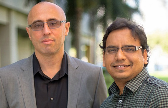
Sakhrat Khizroev, left, with a member of his lab,
researcher Rakesh Guduru
The journal Nanomedicine is featuring the paper by Sakhrat Khizroev, a professor with dual appointments in the Herbert Wertheim College of Medicine and the College of Engineering & Computing.
Using a previously reported FIU-patented technology, researchers began by intravenously administering magneto-electric nanoparticles, or MENs, in mice. With a magnet placed over the head of each subject animal, the particles were pulled through the blood-brain barrier, where they “coupled” the externally created magnetic field with the brain’s intrinsic electric field. This enabled researchers to wirelessly connect their computers and electronics to neurons deep within the brain.
The researchers then sent signals via computer to the MENs, which responded by modulating (or changing from low to high and back again) the frequency of the brain’s naturally occurring electric waves. The resulting pulses created “deep-brain stimulation” that has implications for treating Parkinson’s and other disorders. It stands in contrast to the existing method of deep-brain stimulation, which involves invasive surgery to implant an electrode in the brain and a battery-operated medical device elsewhere in the body.
Worth noting, while the modulation was taking place, researchers had a view of the electrical activity within the brain. This feedback was sent from the MENs to a computer, allowing the researchers to confirm what was taking place.
In a nod to the increasingly personalized nature of medicine, Khizroev believes that MENs could one day be programmed to accomplish any number of medically related procedures to treat various disorders, among them Alzheimer’s and autism. When properly targeted, the particles could, for example, be used to repair cells or destroy plaques. Khizroev also believes that MENs could potentially remain in place within the brain for extended periods to release drugs on a set schedule.
“This study is a critical stepping stone to opening a pathway to understanding the brain and treating many neurodenerative disorders,” Khizroev says. “With this connection, we could see and repair, when necessary, all the electric circuitry deep in the brain.”

Nanoparticles & Food: Vitamins

by Ese Ehimiaghe
For decades, Americans have spent billions of dollars on vitamin and mineral supplements,1and despite concerns about effectiveness and safety,2 a 2013 Gallup poll found that half of Americans take a supplement regularly.3 As nanoparticles have made their way into medicine and pharmaceuticals, they have also moved  into the health supplement industry. In this post, I will explore how nanoparticles are being used in vitamins and supplements.
Vitamins!                        image source
People take vitamins for many different reasons but most often to compensate for compounds whose daily dose they typically cannot meet. While these supplements are supposed to provide the vitamins and nutrients people need, a number of studies have found that some of them can be futile or even harmful.2 Anti-supplement proponents argue that the content of the pills often cannot be absorbed by the body and used for its desired purpose. In the end the compound of interest (in the pill) is filtered through the renal system and ends up in urine.
This concern is one of the reasons nanoparticles are advantageous for the pharmaceutical industry. As mentioned in previous posts (such as here and here), nanoparticles’ shapes can be modified, which means you can make nanotubes or spheres. Those special shapes can carry vitamins and minerals that are often difficult for the body to absorb through traditional mechanisms. The nanoparticles can carry the desired compound through the body so that it gets to its proper location and can be absorbed instead of secreted. This is called increasing the bio-accessibility of the compound.4
In spite of all the good that can come from using nanoparticles in this way there is a certain amount of caution and wariness surround nanoparticles. This is a sensitive topic for two main reasons. First, nanoparticles cannot be seen or tasted in vitamins or supplements. Second,companies in this country are not mandated to label their products that contain nanoparticles. This lack of knowledge makes it difficult for people to take ownership of what goes into their bodies, which makes a lot of people uneasy.5 The lack of openness about nanoparticles also makes people distrustful of the food and drug industry and their motives.
The second major concern with nanoparticles in the food industry relates to the fact that not enough research has been done that looks at how nanoparticles react inside the human body and in the environment. As mentioned above, many people take vitamins and supplements to make up for things they cannot get from their diet or environment. This often means prolonged use of the supplements. However, this leads to important questions about potential use of nanoparticles, such as: Do they change over time? Do they bind to organ lining? Do they react with metals and other chemical species present in the body?
No matter how much we increase the efficiency of supplemental pills, there is still the possibility that the body will excrete some of the materials. This means that we must also ask questions about the environment, like what will happen when the excreted nanoparticles enter our water system? Will the nanoparticles be filtered out during water processing? Will they negatively affect the wildlife and ecosystems around us? How can we track the passage of nanoparticles through different sites and systems?
While there are definitely potential benefits of using nanoparticles in food supplements, there are still many unanswered questions. These are some of the questions that drive the scientific community – including the Center for Sustainable Nanotechnology – to continue our research.

REFERENCES
  1. National Institutes of Health (2013) “Multivitamin/Mineral Supplements” fact sheet for health professionals.
  2. Offit, P. (2013) The Vitamin Myth: Why We Think We Need Supplements. The Atlantic.
  3. Swift, A. (2013) Half of Americans Take Vitamins Regularly. Gallup. 
  4. Liu, Q., Zhang, J., Sun, W., Xie, Q. R., Xia, W., & Gu, H. (2012). Delivering hydrophilic and hydrophobic chemotherapeutics simultaneously by magnetic mesoporous silica nanoparticles to inhibit cancer cells. International Journal of Nanomedicine, 7, 999-1013. doi: 10.2147/IJN.S28088
  5. Kessler, R. (2011). Engineered Nanoparticles in Consumer Products: Understanding a New Ingredient. Environmental Health Perspectives, 119(3), A120-A125. doi:10.1289/ehp.119-a120

terça-feira, 19 de maio de 2015

“Nanotecnologia será a maior revolução que a indústria já viu”


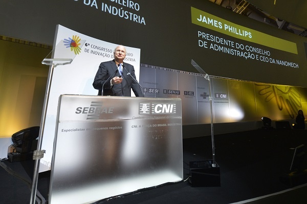
Durante entrevista no 6° Congresso de Inovação da Indústria, ocorrido em São Paulo, o presidente do conselho de administração e CEO da NanoMech, James Phillips, detalhou o que é possível fazer utilizando a novidades nanotecnológicas.

James Phillips - NanoMech


Além do envolvimento com a indústria de nanotecnologia, o executivo, que teve participação em projetos famosos como por exemplo, o que culminou com o sistema de mensagens de texto dos antigos palmtop (PDA), os cabos de modem de internet, o VeinViwer – aparelho que permite a visualização de veias que são muito superficiais ao ultrassom e profundas ao olho nu – e o iPix, considerado, na época, o maior fornecedor do mundo de imagens para internet, em áreas como passeios virtuais, imobiliário online e segurança.

Atualmente, Phillips é presidente do Conselho de Administração e CEO da NanoMech, companhia norte-americana especializada em nanotecnologia que para entender a nanotecnologia é preciso considerar uma escala métrica. “Todo mundo sabe o que é um metro. Nesse caso, nós estamos falando sobre a bilionésima parte de um metro. É escala. A nanotecnologia é a fabricação, construção nessa escala. Um nanômetro é igual uma bola de futebol comparada ao tamanho do planeta. Isso é nano”, conta.

Segundo ele, a nanotecnologia será a maior virada na história da ciência considerando que, por meio dessa escala, pode-se fazer tudo melhor, construir algo melhor, fazer todas as máquinas operarem da melhor forma e de modo mais eficiente. “Com a escala nanométrica é possível fazer novos tipos de equipamentos, novas codificações. Por isso a nanotecnologia vai provocar um efeito profundo tanto na área da saúde, bem como na produção de alimentos, na ciência material especial, quando fazemos qualquer coisa manufaturada podemos fazer melhor. Durante muito tempo, o padrão foi mícron, tamanho que é mil vezes maior do que a escala nano. A escala nano nos possibilita manipular a matéria literalmente”, ilustra.

Dessa forma, as empresas e os profissionais precisam competir mais e precisam assumir riscos se quiserem inovar.”Alguns países e empresas são mais avessos ao risco do que outros. Afinal, inovação requer investimentos adicionais, investimento em tempo, investimento no processo de ideação, de invenção. Depois, é preciso patentear a invenção e isso custa dinheiro”, ressalta.

De acordo com Phillips os países e as empresas devem estar constantemente em estado de renovação, porque é possível estar no comando hoje, mas com o surgimento de um novo algoritmo que pode mudar tudo em termos de comércio. “Pode ser um novo aplicativo que cria um portal totalmente novo para um negócio novo para fazer negócio de forma mais fácil e eficiente. O mundo está se movendo do analógico para o digital em um ritmo incrível, e isso é emocionante porque, quando você se muda para este mundo, consegue fazer tudo mais rápido, melhor e, normalmente, gastando menos. Agora estamos em uma nova transição, da escala mícron para a escala nano”.

Perguntado como vê o Brasil no campo da inovação e também como parceiro de negócios com os Estados Unidos na área tecnológica, o presidente da NanoMech, diz que “ambos são as duas maiores economias do hemisfério ocidental”. Logo, muita gente nos Estados Unidos, não percebe isso. “Eles ainda não se deram conta do fato de que o Brasil tem um incrível senso de inovação e de pioneirismo para realizar coisas novas. Este país é extremamente rico em recursos. Então é importantíssimo que trabalhemos juntos para avançar em tecnologia e inovação. A tecnologia é o reflexo da sociedade. Quase todos os avanços vêm para tornar a vida de todos nós melhor. Eu acho que Brasil e Estados Unidos também devem ter em mente a democracia. Ambos são democracias. E você só tem liberdade de expressar-se e de praticar o seu negócio por meio da democracia. Trabalhar em conjunto é trabalhar por um mundo mais forte”, finaliza.


Fonte: 
B!T magazine

quinta-feira, 7 de maio de 2015

Nanotechnology Environmental Impacts: How much does a free lunch cost?


(This post is written by Dr. Sean McGinnis, Director of the Green Engineering Program at Virginia Tech)
“There is no such thing as a free lunch” goes the old adage.  Applied to technology and the environment, this saying might be “there are always environmental impacts associated with new (and old) technologies.”  One important challenge in a world with limited resources and increasing environmental issues is to consider and assess whether the benefits of a new technology are sufficient to justify the risk of environmental harms.  So let’s explore some ways to estimate the cost of the not-so-free lunch of novel and transformative technologies.
applications vs. environmental impacts
Proponents of nanotechnology claim almost limitless applications and opportunities to improve the lives of people.  To balance this technological optimism, scientists and engineers should remain skeptical and carefully weigh the cost of nanotechnology with the associated environmental risks.
Consider a few examples.  Silver nanoparticles are used as anti-bacterial agents in clothing and medical products to reduce odors and minimize bacterial exposure.  But these nanoparticles also end up in wastewater treatment plants where they can also damage the beneficial bacteria used to clean the wastewater.  Carbon nanotubes and fullerenes can be used for novel electronics, high strength composites, and medical drug delivery.  But the energy required to manufacture and purify these nanomaterials can be orders of magnitude higher compared to current materials.
So, a critical question is: How can we quantify environmental metrics which are robust and transparent?
In recent years, Life Cycle Assessment (LCA) has emerged as a powerful method to quantify environmental impacts.  It is a formal methodology, backed by the International Standards Organization (ISO), to assess a wide variety of environmental impacts including the atmosphere, hydrosphere, biosphere, and human health.
LCA considers environmental impacts for all of the life cycle phases for a product from extraction of raw materials to manufacturing to transportation to use and finally to disposal as shown below:
LCA schematic
Schematic of the LCA Methodology
Analyzing only a portion of the life cycle can lead to incorrect conclusions regarding overall environmental impacts since benefits in one part of the life cycle might be offset by larger issues in another phase. For example, nanocellulose might be biodegradable and less toxic than other materials for use as a drug delivery system, but the environmental burden may be shifted to the strong acids and solvents required for manufacturing.  The boundaries of such analyses must balance the need for a scope that is large enough to include the most significant environmental impacts, but not so large that data collection and analysis is too time-consuming or expensive.
LCA requires a detailed inventory of the inputs from and the outputs to nature for the products, processes or systems being assessed. This inventory typically includes the flows of chemicals, materials, energy and water.  These inputs and outputs must then be translated into environmental impacts.  For example, the same amount of titanium dioxide in bulk form versus nanoscale is likely to have different impacts due to differences in size, surface area, surface coatings, and reactivity.
The amount of environmental damage caused per amount (usually kilograms or liters) of an input or output is known as the characterization factor.  These factors come from research by experts in areas including atmospheric physics, hydrology, soil science, toxicology, and ecology.  The environmental impact of any input or output is the product of the amount of that material (inventory) multiplied by its severity (characterization factor).  By summing the environmental impacts of all inputs and outputs for a product, an overall environmental impact – like a Consumer Report’s score – can be calculated and used for comparisons. (See our earlier post about how environmental impacts are incorporated into environmental rating systems for consumer goods.)
CFC contribute to global warming as well as ozone layer depletionUp to this point, the analysis is objective, using science-based characterization factors and inventory data compiled by industry or individual analysts.  However, to apply these results to decisions, the calculated environmental impacts should be weighted relative to each other for the overall environmental impact score because different stakeholders will not always have the same relative environmental preferences.  For example, some people believe that water quality and availability are more important issues than climate change. 
Or take chlorofluorocarbons (CFCs) for example. CFCs contribute to both global warming as well as ozone layer depletion. The global warming potential (GWP) and the ozone depletion potential (ODP) of CFCs are objective data, measurable in a chemistry lab. But any discussion on whether we should value the impact of CFCs on global warming over its impact on ozone layer depletion (or vice versa) involves subjective preferences.
Therefore, this aspect of LCA is necessarily subjective, though consensus weighting factors have been developed by various scientific groups and organizations.  Because of this subjectivity, weighting is a controversial topic in LCA and it is not allowed by ISO standards for product comparisons in order to avoid bias and conflicts of interest.
Objectivity and subjectivity in LCA
Weighting aside, LCA interpretation issues also include the data uncertainty, time and spatial differences for environmental impacts, and the differences between impact assessment methods.  To address these issues, LCA can use statistical modeling to consider Triple bottom linedifferent design options or to assess the statistical significance of the results given the various uncertainties.  For nanotechnology, there are other specific LCA limitations which will be discussed in a follow-up post (Part 2).
LCA can be used to compare different life cycle phases for the same product or overall impacts for products that perform similar functions, whether or not they use nanotechnology.   However, LCA is not a panacea for decision-making as environmental impacts should be considered along with economic and social metrics, often referred to as the Triple Bottom Line.
LCA does provide a formal metric for data-driven decisions, as opposed to intuition which is prone to errors due to system complexity or other biases.  As a best practice, LCA is used proactively as a design tool for new products in addition to assessing existing products retroactively. This is especially critical for nanotechnology where potential environmental impacts can be much more significant than the materials size or quantities might suggest.