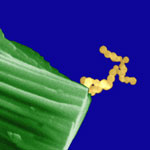
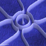
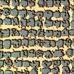
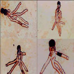
There is a large number of absolutely amazing images out there. Just like the ones below:
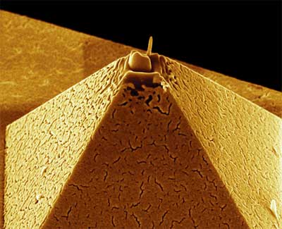
Developing new instruments to be able to "see" at the nanoscale is a research field in itself. Shown here is the tip of an atomic force microscope (AFM), one of the foremost tools for imaging, measuring and manipulating matter at the nanoscale. Here, a platinum electrode measuring one hundredth of a nanometer has been deposited on the tip of this pyramid shaped AFM tip via focused ion beam (FIB) deposition. (Image: C. Menozzi, G.C. Gazzadi, S3 (INFM-CNR), Modena. Artwork: Lucia Covi)
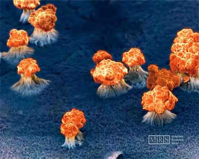
Nano-Explosions – Color-enhanced scanning electron micrograph of an overflowed electrodeposited magnetic nanowire array (CoFeB), where the template has been subsequently completely etched. It’s a reminder that nanoscale research can have unpredicted consequences at a high level. (Image: Fanny Beron, École Polytechnique de Montréal, Canada)
Climatic change on carbon nanotubes – Carbon nanotubes have many characteristics that promise to revolutionize the world of structural materials. There are different ways to grow carbon nanotubes, especially the CVD technique, which allows obtaining SWCNT’s on a silicon surface. These SWCNT can be carried from the silicon surface to another surface, as HOPG, without suffering changes on their properties. That means nanomanipulation of carbon nanotubes. (Mr Miguel Ângel Fernández Vindel, Universidad Autonoma de Madrid/Spain)
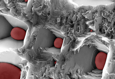
The imaged object is a single crystalline diamond grain that is anisotropically etched by hot spheres of molten nickel (red). Self-organized nickel particles are obtained by sintering a thin Ni film (100 nm) that is evaporated on a polished diamond substrate. Self-organisation and etching are conducted by the following annealing procedure: 1000°C in 500 mbar H2, 24 h. (Image: Waldemar Smirnov, Fraunhofer Institut Angewandte Festkörperphysik, Germany)
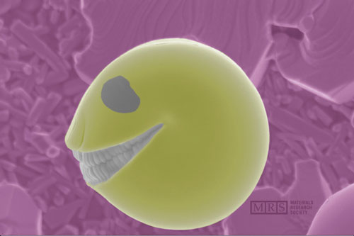
Nano PacMan made of copper oxide. Scanning electron microscope image of a copper oxide cluster, 3.5 microns in diameter, prepared by evaporation and condensation over an alumina substrate. The smiley nose and eye are present in the original SEM image, which has only been color-enhanced. (Image: Elisabetta Comini, University of Brescia, Italy)
We have a collection of these amazing images in some of our articles. You can find them here:
Fonte: NanoWerk