| Almost three years ago a team of scientists at the U.S. Department of Energy's Lawrence Berkeley National Laboratory (Berkeley Lab) was performing an experiment in which layers of gold mere nanometers thick were being heated on a flat silicon surface and then allowed to cool. They watched in surprise as peculiar features expanded and changed on the screen of their electron microscope, finally settling into circles surrounded by irregular blisters. | |
| The circles varied in diameter up to a few millionths of a meter, and in the center of each was a perfect square. The mysterious patterns were reminiscent of nothing so much as so-called "alien" crop circles. | |
| Au (100nm) / native SiO2 / Si (100), annealed at 600C, imaged with in situ SEM, showing formation of eutectic circles. | |
| Until recently the cause of these strange formations remained a mystery. Now theoretical insights have explained what's happening, and the results have been published online by Physical Review Letters("Large Reaction Rate Enhancement in Formation of Ultrathin AuSi Eutectic Layers"). | |
| Eagerly melting alloys | |
| When two solids are combined in just the right proportions, changes in chemical bonding may produce an alloy that melts at a temperature far lower than either can melt by itself. Such an alloy is called eutectic, Greek for "good melting." The eutectic alloy of gold and silicon – 81 percent gold and 19 percent silicon – is especially useful in processing nanoscale semiconductors such as nanowires, as well as for device interconnections in integrated circuits; it liquefies at a modest 363° Celsius, far lower than the melting point of either pure gold, 1064°C, or pure silicon, 1414°C. | |
| "Gold-silicon eutectic liquid can safely solder chip layers together or form microscopic conducting wires, by flowing into channels in the substrate without burning up the surroundings," says Berkeley Lab's Junqiao Wu. "It's particularly interesting for processing nanoscale materials and devices." Wu cites the example of silicon nanowires, which can be grown from beads of eutectic liquid that form from droplets of gold. The beads catalyze the deposition of silicon from a chemical vapor and ride atop continually lengthening nanowire whiskers. | |
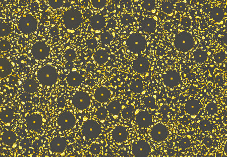 | |
| When a thin layer of gold anneals on top of a silicon wafer coated with native silicon oxide, randomly distributed pools of eutectic alloy quickly form – and then go through a rapid series of strange changes, leaving behind bare silicon-dioxide circles surrounded by debris. Each denuded circle reveals a perfect square at its center. The area shown is about 107 by 155 micrometers. | |
| Understanding just how and why this happens has been a challenge. Although eutectic alloys are well studied as solids, the liquid state presents more obstacles, which are particularly formidable at the nanoscale because of greatly increased surface tension – the same surface forces that make it difficult to form ultra-thin films of water, for example, because they pull the water into droplets. At smaller scales the ratio of surface area to bulk increases markedly, and nanoscale structures have been described as virtually "all surface." | |
| These are the conditions that the team led by Wu, who is a faculty scientist in Berkeley Lab's Materials Sciences Division and a professor in the Department of Materials Science and Engineering at the University of California at Berkeley, set out to examine, by creating the thinnest possible films of gold-silicon eutectic alloys. The researchers did so by starting with a substrate of pure silicon, on whose flat surface an extremely thin barrier layer (two nanometers thick) of silicon dioxide had formed. On this surface they laid layers of pure gold, varying the thickness from one trial to the next between just a few nanometers to a hefty 300 nanometers. The silicon dioxide barrier prevented the pure silicon from mixing with the gold. | |
| The next step was to heat the layered sample to 600°C for several minutes – not hot enough to melt the gold or silicon but hot enough to cause naturally existing pinholes in the thin silicon dioxide layer to enlarge into small weak spots, through which pure silicon could come in contact with the overlying gold. At the high temperature, silicon atoms quickly diffused out of the substrate and into the gold, forming a layer of eutectic gold-silicon alloy nearly the same thickness as the original gold and spreading in a virtually perfect circle from the central pinhole. | |
| When the circular disk of eutectic alloy got large enough it suddenly broke up, disrupted by the high surface energy of the gold-silicon eutectic liquid. The debris was literally pulled to the edges of the disk, piling up around it to leave a central denuded zone of bare silicon dioxide. | |
| In the center of the denuded zone, a perfect square of gold and silicon remained. | |
| Chemistry and crystallography, not aliens | |
| The researchers' most surprising discovery was that the thinner the original gold layer, the faster the eutectic circles expanded. The reaction rate when the gold layers were only 20 nanometers thick was more than 20 times faster than when the layers were 300 nanometers thick. And while at first glance the dimensions of the gold and silicon squares inside the circular denuded zones seemed variable, there was in fact a strict relation between the size of the square and the size of the circle: the radius of the circle was always the length of the square raised to the power of 3/2. | |
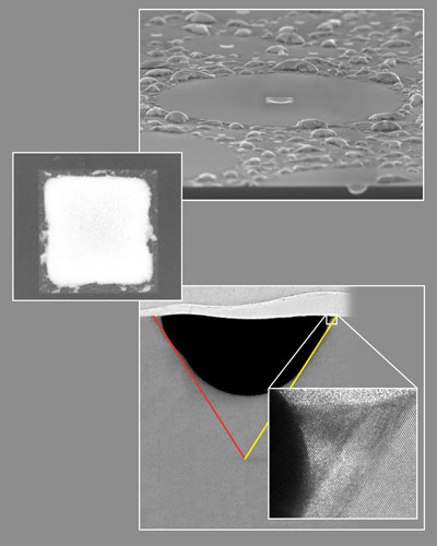 | |
| The denuded zone and central square (top and center): at bottom, a side view reveals the structure beneath the square, a pyramid whose sides lie along the low-energy planes of the silicon substrate. After separation upon cooling, the gold has retreated (dark gray). A layer of regrown silicon is visible in the high-resolution inset image, precisely following the crystal planes of the substrate shown at far right. | |
| How did the squares get there in the first place? They originated as weak spots that were the sources of the spreading eutectic gold-silicon circles; when the circular eutectic was ruptured the squares filled with the same eutectic, which remained at the centers of the denuded zones. As they cooled, the gold and silicon within the squares separated, leaving sharply defined edges that were pure silicon; the centers were more roughly outlined squares of pure gold. | |
| By slicing through the silicon/silicon dioxide/gold layercake and looking sideways at the structures with an electron microscope, the researchers found that the surface squares were the bases of inverted pyramids, resembling teeth penetrating the thin silicon dioxide layer and embedded in the silicon wafer. The squares were square, in fact, because of the silicon's orientation: the substrate had been cut along the crystal plane that defined the base. The four triangular sides of the pyramids lay along the low-energy planes of the crystal lattice and were defined by their intersections. | |
| What began as a puzzling phenomenon reminiscent of "The X Files," if on a considerably smaller scale than the cosmic, the mystery of the "nanoscale crop circles" eventually yielded to careful observation and theoretical analysis – despite the obstacles posed by high temperatures, nanoscale sizes, instabilities of the liquid state, and extremely rapid time scales. | |
| "We found that the reaction rate in forming small-sized gold-silicon eutectic liquids – and perhaps in many other eutectics as well – is dominated by the thickness of the reacting layers," says Wu. "This discovery may provide new routes for the engineering and processing of nanoscale materials." Fonte: NanoWerk |